An interface that has emerged to meet these growing demands is SLVS-EC (Scalable Low-Voltage Signaling with Embedded Clock), a proprietary interface developed by Sony. Early-generation sensors could easily transmit data over simple parallel interfaces or low-speed differential links, but the data output of modern sensors has grown exponentially. A sensor such as Sony’s IMX811, with its 247MP, generates data rates close to 40Gbps at 12.4fps, and 12-bit depth. Such data volumes require sophisticated and high-speed transmission protocols.
Different Data Interfaces
Several interfaces have emerged over time to fulfill these transmission needs, each with its own strengths and limitations. Traditional interfaces like LVDS (Low-Voltage Differential Signaling) and its derivatives, Sub-LVDS and SLVS, are widely used in industrial and consumer applications. Although these interfaces are effective, they are limited in their bandwidth and typically support data volumes in the range of hundreds of megabits per second per channel.
In contrast, the MIPI CSI-2 interface became the de facto standard for mobile and embedded applications. Originally developed for smartphones, MIPI CSI-2 offers greater speeds, up to 4.5Gbps per lane with D-PHY and even higher with C-PHY. CSI-2 has the advantage of being widely supported by a variety of chip sets and processors, making it a versatile option. However, it too has limitations when it comes to transmitting uncompressed ultra-high-resolution video streams at high frame rates, particularly in systems that require long cable lengths or robust noise immunity.
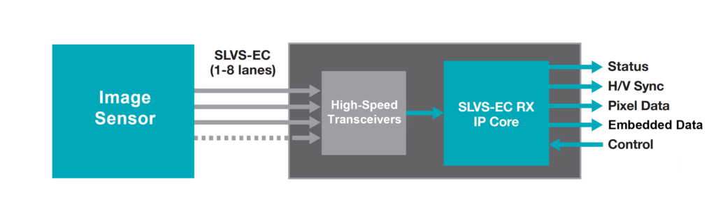
These limitations led to the development of SLVS-EC by Sony, Introduced as a high-speed, scalable interface specifically for high-resolution and high-speed industrial and professional imaging applications. EC (Embedded Clock) refers to one of its core innovations: it embeds the clock signal directly within the data stream. This eliminates the need for separate clock lanes and drastically reduces the risk of signal skew, making it far more robust over longer distances or in electrically noisy environments. SLVS-EC is also highly scalable. Depending on system requirements, designers can use anywhere from a single data lane to eight lanes, each capable of transferring data at speeds ranging from 1.15 to 10Gbps. In 2025 version 3.1 of the SLVS-EC standard has been released allowing up to sixteen lanes with each capable of transferring up to 12.5Gbps of data. For example, Sony’s new IMX926, with 12.4MP at 589fps, produces approximately 80Gbps at 10-bit depth. This amount of data can only be managed by SLVS-EC, and it just requires eight lanes at 12.5Gbps using v3.1 of the standard.
PCB Designs & Power Management
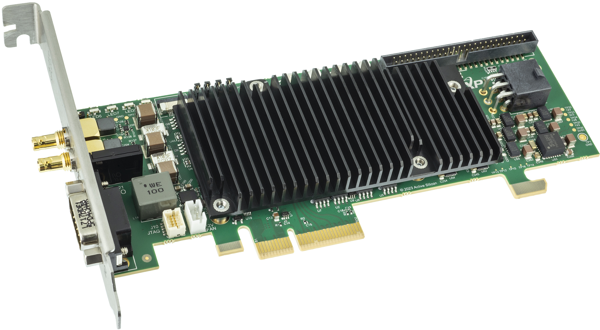
As the resolution and speed of image sensors increase, so do the demands on data throughput, power management, and thermal performance. In addition to sheer data rate, the integration of such sensors presents challenges across the board. High-resolution and high-speed sensors generate heat that must be dissipated without introducing instability or artifacts. This is where SLVS-EC proves its worth again. By eliminating the need for an external clock, drastically reducing the number of lanes, simplifying trace routing, and reducing the number of pins required for high-bandwidth transmission, it becomes much easier to design PCBs with thermal vias or heat sinks that are mechanically and thermally robust. Moreover, SLVS-EC supports features like error correction and cyclic redundancy checks, which enhance data integrity during high-speed transmissions.
Conclusion
SLVS-EC has emerged not simply as another option on a list of data interfaces, but as a technological necessity for certain high-end applications. It fills the gap between lower-cost, lower-speed consumer interfaces and the heavy throughput generated by modern sensors for modern applications. The interface’s combination of embedded clocking, high throughput, low voltage transmission, serviceability for longer cables, and lane scalability makes it ideally suited for the next generation of image sensors. And with newer versions pushing per-lane speeds beyond 12Gbps and adding increasingly sophisticated error handling, its future looks promising. While SLVS-EC may not replace every interface currently in use, it serves a vital role in industrial and scientific imaging, where reliability, bandwidth, and design flexibility are paramount.